Wave soldering is a great process for multiple component soldering, an automated production method enabling small to large PCBs with 100’s and often 1000's of joints to be soldered in seconds compared to labour-intensive hand soldering. A tried and tested long-established process, wave soldering involves the fluxing, pre-heating, and finally wave soldering of the board on a conveyor system.
Great - so we have our circuit board, populated with through-hole (PTH) components, and maybe SMT components there as well. You've ensured all the components have been placed, the orientation of parts is right, and you've considered any plated fixing holes and components that maybe you don't want to solder (kapton polyimide tapes and dots and peelable solder masks are great for this).
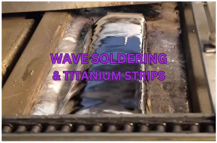
THE WAVE - Your PCB, with all the costs involved from the bare board, all the components, and the labour populating the parts, is now heading for the bath of molten solder in the region of 260 - 270C. It would have travelled through a pre-heat section warming the parts up from ambient to eliminate any thermal shock.
PROBLEM - You see the board start to sag as the PCB laminate, with the weight of components, meets the solder. You see molten solder start to flow over the front edge of the PCB! You see that flowing solder covering areas of the board! You see molten solder flowing over the trailing edge of the board and into the wave solder machine!
Been there, done that, and have the t-shirt! A health and safety nightmare - molten solder is very dangerous, no two ways about it!
CONSIDERATIONS
- The PCB size - the longest dimension is best supported by the wave solder pallet or conveyor's fingers, so it is the width to consider
- The PCB thickness - for laminates of 2mm and greater, then the problem is very much less compared to a typical laminate of 1.60mm. Even thinner well the problem gets greater
- Component weights - Are you soldering transformers, heatsinks or parts that are making the board heavy?
- PCB rigidity and routed profiles - If your board is a motherboard panel, then if each PCB is routed, rather than scored, this will make the panel less rigid.
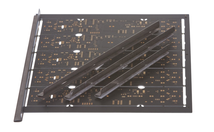
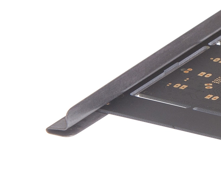
A SIMPLE ANSWER - Titanium strips, or titanium ploughs, are simply a strip of metal that has a profile designed to push on over the front leading edge of the PCB. I'd suggest also placing one at the back trailing edge to help support the panel. Titanium is TOUGH! - It can comfortably handle the very high temperatures for the soldering process.
TITANIUM STRIPS - At Somerset Solders, we stock a range of titanium plough lengths from 100mm to 310mm long, and though the standard strips are stocked for 1.60mm PCB laminate, different thicknesses can be fabricated to order. Custom lengths up to 310mm are also available.

